Products
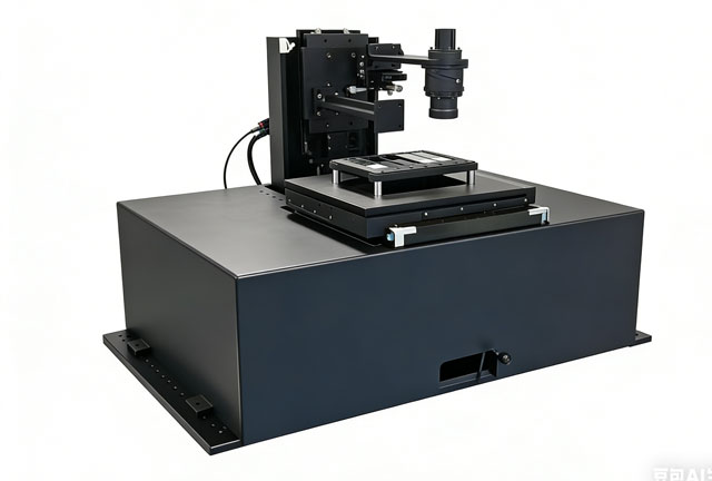
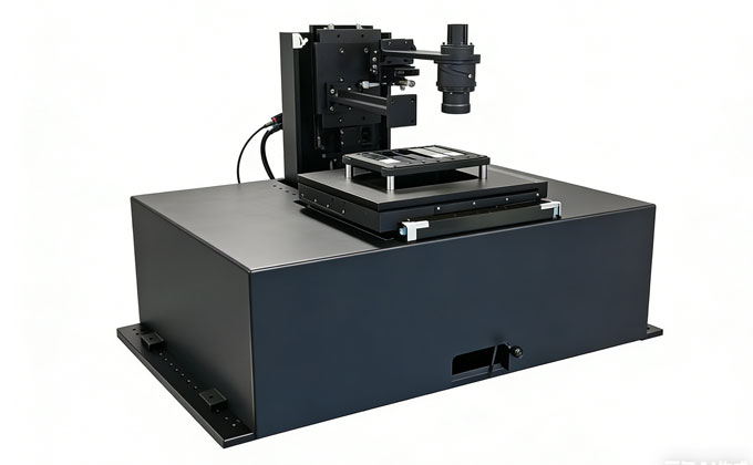
TerraScope™Ultra
Unified Broadband 3D Terahertz Platform for Extreme-Range Carrier, 2DEG & Full-Wafer Semiconductor Intelligence.
Product Parameters
1.The Broadband Solution: Extreme-Range Carrier Profiling for Next-Generation Semiconductors: Unprecedented dynamic range; Adaptive frequency engine for optimized sensitivity across doping regimes
2.The Multi-Layer Solution: Non-Destructive 3D Mapping of Complex Epitaxial Stacks: Full-stack parameter decoupling;Sub-nanometer interface sensitivity;Automated thickness–carrier concurrency correction
3.The 2DEG & Advanced Materials Solution: Beyond Bulk Characterization;Direct 2DEG characterization;Anisotropy-resolved measurements;Polytype differentiation (e.g., wide-bandgap materials)
4.The High-Speed Production Solution: Real-Time, 100% Wafer Inspection for Power Electronics;Unmatched measurement speed;True non-contact operation;Compatible with conductive and semi-insulating materials;In-situ integration capability for production environments
5.Mastering the Complexities of Modern Semiconductor Physics: Multi-Model Fitting Framework; Seamlessly switch between Drude, Drude–Smith, Drude–Lorentz, and specialized thin-film models within a single unified interface.
6.Comprehensive Reporting: Beyond carrier concentration (N) and mobility (μ), the system provides; Confidence intervals; Fit quality indicators; Automated identification of physical phenomena (e.g., multi-phonon interference detected and filtered)
Technical Specifications
Parameter | Performance |
Carrier Concentration Range | 1012-1020cm-3 |
Mobility accuracy | +-5%(calibrated) |
Thickness Resolution | <1nm |
Measurement Speed | <5 sec/point |
Wafer Compatibility | Si, GaAs,GaN,SiC,etc |
Semiconductor Material Testing Parameters and Standards
The following table compares key testing parameters and standards for major semiconductor materials, optimized for terahertz technology characteristics:
Material Type | Key Testing Parameters | Terahertz Technology Advantages | Industry Standards Reference |
Silicon (Si) | - Carrier concentration (1e14 1500 cm²/V·s) | Rapid full-wafer scanning | SEMI MF1725 |
Silicon Carbide (SiC) | - 4H/6H polytype differentiation | Wide bandgap material penetration | JEDEC JC70 |
Gallium Nitride (GaN) | - Polarization field strength (0.1~5 MV/cm) | Non-contact piezoelectric response measurement | IEEE 1620 |
Gallium Arsenide (GaAs) | - Doping gradient (1e16~1e19 cm⁻³) | Picosecond time resolution | MIL-PRF-19500 |
Beta-Gallium Oxide (β-Ga₂O₃) | - Deep level defects (>0.5eV) | Terahertz absorption fingerprinting | EIAJ ED-7301 |
Technical Specifications:
Measurement accuracy exceeds ±3% compared to conventional Hall effect tests
Supports full 300mm wafer automated mapping (ASTM F1526)
Data output complies with SECS/GEM protocol
(Custom testing solutions available for different process nodes)
-
Previous
TERA X1

-
Next
none_found


Related Solutions


Related News

AI-Powered Terahertz Inspection Platform Exclusively for Aerospace MRO---TERA X1
Built specifically for aerospace aircraft maintenance scenarios, it leverages terahertz non-destructive testing principles to accurately measure coating thickness and detect hidden defects in multi-layer structures at an early stage, safeguarding aircraft safety.
Continue Reading

Introducing TerraScope™ Ultra: 3D Terahertz Intelligence at the Wafer Scale
TerraScope™ Ultra:Unified Broadband 3D Terahertz Platform for Extreme-Range Carrier, 2DEG & Full-Wafer Semiconductor Intelligence
Extreme-Range Carrier Analysis: Precisely maps carrier density, mobility, and lifetime across various doping levels and multilayer structures with high resolution and deep penetration.
Continue Reading