News
02
March
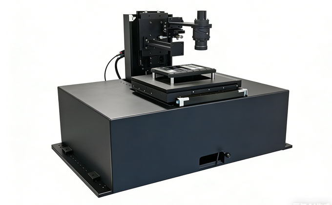
Introducing TerraScope™ Ultra: 3D Terahertz Intelligence at the Wafer Scale
TerraScope™ Ultra:Unified Broadband 3D Terahertz Platform for Extreme-Range Carrier, 2DEG & Full-Wafer Semiconductor Intelligence
Extreme-Range Carrier Analysis: Precisely maps carrier density, mobility, and lifetime across various doping levels and multilayer structures with high resolution and deep penetration.
2DEG Intelligence: Provides direct, non-contact visualization and quantification of Two-Dimensional Electron Gas uniformity and properties in heterostructures, critical for HEMT and quantum devices.
Full-Wafer Semiconductor Intelligence: Delivers high-throughput 3D tomographic scans across entire wafers, revealing critical parameters like resistivity, layer thickness, and defects to accelerate R&D and enhance process control.


